Words of Wisdom:
"to rid yourself of desire to be empty to attain enlightment"
- Gautam
Essay
- Date Submitted: 10/09/2014 12:25 AM
- Flesch-Kincaid Score: -52.4
- Words: 1345
- Essay Grade: no grades
- Report this Essay
8085 Architecture & 8085 Architecture & Its Assembly language programming
Dr A Sahu Dept of Computer Science & Engineering Engineering IIT Guwahati
Outline
• 8085 Era and Features • 8085
– Block diagram (Data Path) – Bus Structure – Register Structure g
• Instruction Set of 8085 • Sample program of 8085 Sample program of 8085 • Simulator & Kit for 8085
8085 Microprocessor 8085 Microprocessor
• • • • • • • • 8 Bit CPU 3‐6Mhz Simpler design: Single Cycle CPU p g g y ISA = Pre x86 design (Semi CISC) 40 Pin Dual line Package 40 Pin Dual line Package 16 bit address 6 registers: B, C, D, E, H,L Accumulator 8 bit
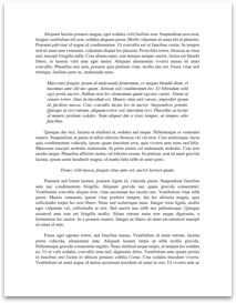
8085 Microprocessor Architecture
ReSeT6.5 INTR INTA RST5.5 RST7.5 TRAP SID SOD
Interrupt Control Bus 8 Bit ACC tmp R Flag I Decode I Decode & M/C Encodin g
Serial I/O Control
MUX IR W B D H SP PC
Inc/Dec. ter / Add latch
Z C E L
ALU
Timing and Control
Add Buff
Data/Add Buff
The 8085 Bus Structure
A15 A0 Address Bus (16bit)
Memory 8085 MPU
I/P O/P
D7 D0
Data Bus (8bit) Control Bus (8bit)
8085 Bus Structure
• Address Bus : Consists of 16 address lines: A0 – A15 Address Bus : Consists of 16 address lines: A
– Address locations: 0000 (hex) – FFFF (hex) – Can access 64K ( = 216 ) bytes of memory, each byte has 8 bits ( ) y y, y
– Can access 64K × 8 bits of memory – Use memory to map I/O, Same instructions to use for accessing I/O devices and memory /
• Data Bus : Consists of 8 data lines: D0 – D7
–O Operates in bidirectional mode t i bidi ti l d – The data bits are sent from the MPU to I/O & vice versa – Data range: 00 (hex) – FF (hex) Data range: 00 (hex) – FF (hex)
• Control Bus:
– Consists of various lines carrying the control Consists of various lines carrying the control signals such as read / write enable, flag bits
8085 Registers
• Registers:
– Six general purpose 8‐bit registers: B, C, D, E, H,L – Combined as register pairs to perform 16‐bit ...
Dr A Sahu Dept of Computer Science & Engineering Engineering IIT Guwahati
Outline
• 8085 Era and Features • 8085
– Block diagram (Data Path) – Bus Structure – Register Structure g
• Instruction Set of 8085 • Sample program of 8085 Sample program of 8085 • Simulator & Kit for 8085
8085 Microprocessor 8085 Microprocessor
• • • • • • • • 8 Bit CPU 3‐6Mhz Simpler design: Single Cycle CPU p g g y ISA = Pre x86 design (Semi CISC) 40 Pin Dual line Package 40 Pin Dual line Package 16 bit address 6 registers: B, C, D, E, H,L Accumulator 8 bit
8085 Microprocessor Architecture
ReSeT6.5 INTR INTA RST5.5 RST7.5 TRAP SID SOD
Interrupt Control Bus 8 Bit ACC tmp R Flag I Decode I Decode & M/C Encodin g
Serial I/O Control
MUX IR W B D H SP PC
Inc/Dec. ter / Add latch
Z C E L
ALU
Timing and Control
Add Buff
Data/Add Buff
The 8085 Bus Structure
A15 A0 Address Bus (16bit)
Memory 8085 MPU
I/P O/P
D7 D0
Data Bus (8bit) Control Bus (8bit)
8085 Bus Structure
• Address Bus : Consists of 16 address lines: A0 – A15 Address Bus : Consists of 16 address lines: A
– Address locations: 0000 (hex) – FFFF (hex) – Can access 64K ( = 216 ) bytes of memory, each byte has 8 bits ( ) y y, y
– Can access 64K × 8 bits of memory – Use memory to map I/O, Same instructions to use for accessing I/O devices and memory /
• Data Bus : Consists of 8 data lines: D0 – D7
–O Operates in bidirectional mode t i bidi ti l d – The data bits are sent from the MPU to I/O & vice versa – Data range: 00 (hex) – FF (hex) Data range: 00 (hex) – FF (hex)
• Control Bus:
– Consists of various lines carrying the control Consists of various lines carrying the control signals such as read / write enable, flag bits
8085 Registers
• Registers:
– Six general purpose 8‐bit registers: B, C, D, E, H,L – Combined as register pairs to perform 16‐bit ...
Comments
Express your owns thoughts and ideas on this essay by writing a grade and/or critique.
Sign Up or Login to your account to leave your opinion on this Essay.
Copyright © 2024. EssayDepot.com
No comments